Knowledge Base
Semiconductor Test & Measurement Solutions: Precision for Semiconductor Excellence

Overview
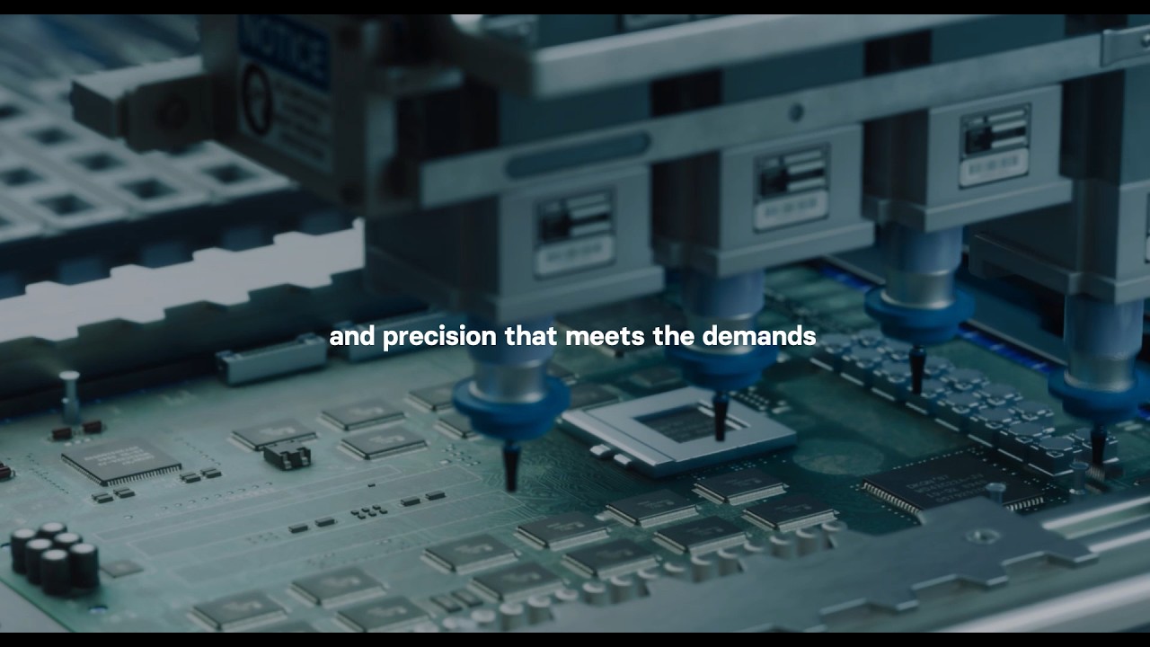
Industrial Physics delivers test and measurement solutions built for the demands of advanced semiconductor manufacturing. In this video, you’ll see how trace oxygen analysis at the 2 ppm level, non-contact coating thickness measurement, and precision testing across SMT ovens, TCB equipment, vacuum chambers, and advanced packaging processes enable the accuracy that makes mass production of next-generation chips possible.
Key Testing Capabilities for Semiconductors
- Trace oxygen analysis at the 2 ppm level (EC913 and ZR810 series)
- Gas analysis for inert atmospheres and vacuum chamber purity
- Non-contact coating thickness measurement (0.2 to 250 microns)
- Optical testing for coating transparency and film clarity
- Contact angle testing for surface wettability and cleanliness
- Salt spray corrosion testing for electronic components
- Air and vacuum leak testing to IP67 sealing requirements
- Temperature and climatic tracking for reflow and curing
- Technology from SpecMetrix, TQC Sheen, Systech, C&W, and TME
What You’ll Learn in This Video
- 00:00 – Introduction to semiconductor manufacturing quality control
- 00:08 – Why oxygen contamination and process precision matter
- 00:22 – Overview of the testing solutions portfolio
- 01:15 – Advanced packaging expertise and global service support
Critical Testing for Semiconductor Manufacturing
In semiconductor manufacturing, oxygen contamination means oxidation, failed bonds, and compromised yields that cost millions. When you’re producing next-generation chips at the cutting edge of technology, precision is the difference between successful mass production and costly failures.
Industrial Physics provides trace oxygen analysis at the 2 ppm level, non-contact coating thickness measurement, and precision testing across the processes that define advanced chip production. From SMT ovens and TCB equipment to vacuum chambers and advanced packaging, this enables chip manufacturers, equipment OEMs, and electronics assembly operations to maintain the accuracy required for mass production of next-generation chips.
Typical Applications
- Advanced chip and logic manufacturing
- SMT and TCB equipment processes
- Advanced packaging and thin film deposition
- Electronics assembly and component sealing
- Equipment OEMs and R&D laboratories
Technical Summary
- Test parameters: Trace oxygen (2 ppm level), gas analysis, coating thickness (0.2-250 microns), optical, contact angle, corrosion (salt spray), air/vacuum leak (IP67), temperature/climatic
- Named products: EC913 and ZR810 oxygen analysers, SpecMetrix thickness systems, Fibro PGX+ contact angle tester, C&W salt spray chambers, TME Worker leak systems, TQC Sheen oven trackers
- Standards: IP67 sealing referenced; no other specific standards stated – confirm before adding
- Brands: SpecMetrix, TQC Sheen, Systech, C&W, TME
To explore more, visit the campaign page.
Speak With an Expert
If you’re looking to maintain the precision required for advanced semiconductor production, our team is here to support you. Contact our experts today.
Was this useful?
Related Videos
-

Overview Industrial Physics delivers test and measurement solutions built for the demands of advanced semiconductor manufacturing. In this video, you'll see how trace oxygen analysis at the 2 ppm level, non-contact coating thickness measurement, and precision testing across SMT ovens, TCB equipment, vacuum chambers, and advanced packaging processes enable the accuracy that makes mass production…
-

Overview The Systech EC900 Process Oxygen Analyser is a high-performance electrochemical oxygen analyser designed for continuous oxygen process analysis in industrial gas streams and atmospheres. In this video, you’ll see how the EC900 operates, what makes it a reliable choice for quality control and process monitoring teams, and how its patented sensor technology delivers accurate, low-maintenance oxygen measurement down to 20ppm from ambient air in two…
-

Overview The Systech ZR800 Oxygen Analyzer is a high-performance, continuous oxygen analysis system designed for demanding industrial process environments. In this video, you’ll see how the ZR800 operates, what makes it a trusted solution for quality control, process monitoring, and safety applications, and how its zirconia sensor technology delivers ultra-fast, accurate oxygen measurement across a wide range of industrial gas streams. Key…
